

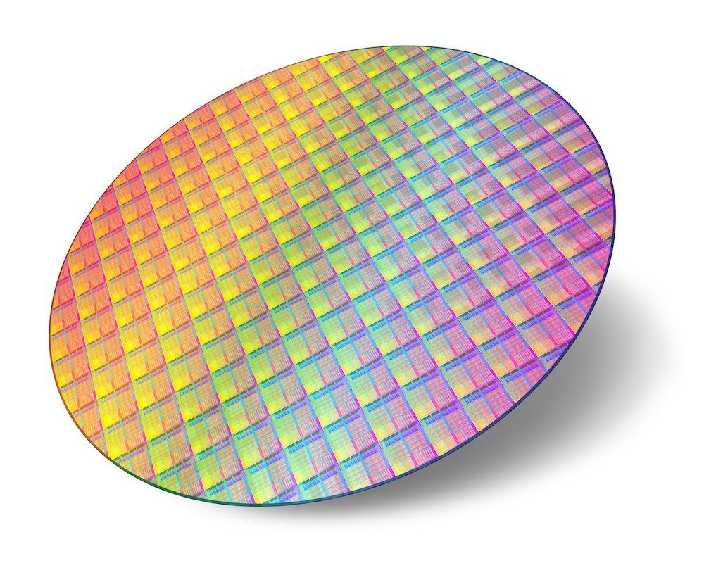
Semiconductor Fabrication Products
Semiconductor Fabrication Products
Semiconductor Fabrication Products
End-Point Control for CMP Processes
End-Point Control forCMP Processes
End-Point Control for CMP Processes
M17 provides a solution for a wide range of complex problems associated with CMP process control. This has been used successfully in manufacturing and development lines worldwide since 1996.
The basic approach to control a CMP process containing a nitride change at the stoplayer is the foundation of this M17 system. M17 has been developed jointly by ECO PHYSICS and a leading edge semiconductor company in 1996.
M17 provides a solution for a wide range of complex problems associated with CMP process control. This has been used successfully in manufacturing and development lines worldwide since 1996.
The basic approach to control a CMP process containing a nitride change at the stoplayer is the foundation of this M17 system. M17 has been developed jointly by ECO PHYSICS and a leading edge semiconductor company.
M17, the system that provides highly sensitive and reliable closed loop control for applications such as STI and BP.
The Challenge
Existing methods to control CMP-processes are either based on simple timing, on frictional change, on optical measurement of thickness or on measurement control in-line or off-line. All these methods need a relatively large process window. CMP processes depend on quite a large number of parameters such as downward pressure, rotational speed of the platen and the carrier, relative rotational directions, kind and condition of the pad, slurry, temperature and much more.
For STI all above parameters are changing. STI has also a very small process window, so the methods mentioned above are poorly suited or very time consuming.
The big challenge has been for many years:
- to fully automate the CMP process by a system including an in-situ sensor which, in real-time, precisely detects the actual polishing position to stop the process;
- to develop a method which is independent of all the mentioned parameters;
- to develop a simple tool which upgrades current and future CMP machines to the latest, most efficient automation technique.
The Solution has the simple name: M17.
M17 is based on a process-state technology measuring the whole wafer and therefore delivers a representative signal for active structures at the chip. This non-intrusive system measures polishing progress in-situ and in real-time, independent of any kind of removal rate variations. M17 stops the CMP process precisely on layers containing a nitride change. It is designed to run round the clock with minimum maintenance (a few hours a year). It drastically reduces and, in many cases completely eliminates, the measurement of incoming and post CMP wafer thickness. This results in drastic increase of throughput and almost eliminates any over- or underpolish, enhancing process yield. Both features give tremendous savings.
The system is basically so reliable because it measures the light emitted as a result of chemical reactions occurring during the polishing process and in the M17 itself.
M17 is also an effective tool to develop new processes.
CONTACT US TODAY!
M17, the system that provides highly sensitive and reliable closed loop control for applications such as STI and BP.
M17 Series Overview
The Challenge
Existing methods to control CMP-processes are either based on simple timing, on frictional change, on optical measurement of thickness or on measurement control in-line or off-line. All these methods need a relatively large process window. CMP processes depend on quite a large number of parameters such as downward pressure, rotational speed of the platen and the carrier, relative rotational directions, kind and condition of the pad, slurry, temperature and much more.
For STI all above parameters are changing. STI has also a very small process window, so the methods mentioned above are poorly suited or very time consuming.
The big challenge has been for many years:
- to fully automate the CMP process by a system including an in-situ sensor which, in real-time, precisely detects the actual polishing position to stop the process;
- to develop a method which is independent of all the mentioned parameters;
- to develop a simple tool which upgrades current and future CMP machines to the latest, most efficient automation technique.
The Solution has the simple name: M17.
M17 is based on a process-state technology measuring the whole wafer and therefore delivers a representative signal for active structures at the chip. This non-intrusive system measures polishing progress in-situ and in real-time, independent of any kind of removal rate variations. M17 stops the CMP process precisely on layers containing a nitride change. It is designed to run round the clock with minimum maintenance (a few hours a year). It drastically reduces and, in many cases completely eliminates, the measurement of incoming and post CMP wafer thickness. This results in drastic increase of throughput and almost eliminates any over- or underpolish, enhancing process yield. Both features give tremendous savings.
The system is basically so reliable because it measures the light emitted as a result of chemical reactions occurring during the polishing process and in the M17 itself.
M17 is also an effective tool to develop new processes.
CONTACT US TODAY!
M17, the system that provides highly sensitive and reliable closed loop control for applications such as STI and BP.
The Challenge
Existing methods to control CMP-processes are either based on simple timing, on frictional change, on optical measurement of thickness or on measurement control in-line or off-line. All these methods need a relatively large process window. CMP processes depend on quite a large number of parameters such as downward pressure, rotational speed of the platen and the carrier, relative rotational directions, kind and condition of the pad, slurry, temperature and much more.
For STI all above parameters are changing. STI has also a very small process window, so the methods mentioned above are poorly suited or very time consuming.
The big challenge has been for many years:
- to fully automate the CMP process by a system including an in-situ sensor which, in real-time, precisely detects the actual polishing position to stop the process;
- to develop a method which is independent of all the mentioned parameters;
- to develop a simple tool which upgrades current and future CMP machines to the latest, most efficient automation technique.
The Solution has the simple name: M17.
M17 is based on a process-state technology measuring the whole wafer and therefore delivers a representative signal for active structures at the chip. This non-intrusive system measures polishing progress in-situ and in real-time, independent of any kind of removal rate variations. M17 stops the CMP process precisely on layers containing a nitride change. It is designed to run round the clock with minimum maintenance (a few hours a year). It drastically reduces and, in many cases completely eliminates, the measurement of incoming and post CMP wafer thickness. This results in drastic increase of throughput and almost eliminates any over- or underpolish, enhancing process yield. Both features give tremendous savings.
The system is basically so reliable because it measures the light emitted as a result of chemical reactions occurring during the polishing process and in the M17 itself.
M17 is also an effective tool to develop new processes.
CONTACT US TODAY!
REQUEST A BROCHURE
Please e-mail the Medical Product Manager, [email protected]
, or the Industrial Product Manager, [email protected]
for more information on ECO PHYSICS, Inc. products, or call us at 734.998.1600
REQUEST A BROCHURE
Please e-mail the Medical Product Manager, [email protected]
, or the Industrial Product Manager, [email protected]
for more information on ECO PHYSICS, Inc. products, or call us at 734.998.1600
UPCOMING EVENTS
Please go to our ABOUT US section for the latest updates.
REQUEST A BROCHURE/QUOTE
Please e-mail the Medical Product Manager, [email protected]
, or the Industrial Product Manager, [email protected]
for more information on ECO PHYSICS, Inc. products, or call us at 734.998.1600
SIGN UP FOR OUR QUARTERLY NEWSLETTER
Thank you for contacting us.
We will get back to you as soon as possible.
We will get back to you as soon as possible.
Oops, there was an error sending your message.
Please try again later.
Please try again later.
ECO PHYSICS, INC.
3915 Research Park Drive, Suite A-3
Ann Arbor, Michigan 48108-2200
ECO PHYSICS, INC.
3915 Research Park Drive, Suite A-3
Ann Arbor, Michigan 48108-2200